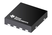
Datasheet Texas Instruments TPS61045DRBT — 数据表
| 制造商 | Texas Instruments |
| 系列 | TPS61045 |
| 零件号 | TPS61045DRBT |

QFN-8中具有28V,85%效率的升压转换器,数字可调8-SON -40至85
数据表
TPS61045 Digitally Adjustable Boost Converter datasheet
PDF, 1.1 Mb, 修订版: C, 档案已发布: Dec 5, 2014
从文件中提取
价格
状态
| Lifecycle Status | Active (Recommended for new designs) |
| Manufacture's Sample Availability | No |
打包
| Pin | 8 |
| Package Type | DRB |
| Industry STD Term | VSON |
| JEDEC Code | S-PDSO-N |
| Package QTY | 250 |
| Carrier | SMALL T&R |
| Device Marking | BHT |
| Width (mm) | 3 |
| Length (mm) | 3 |
| Thickness (mm) | .88 |
| Pitch (mm) | .65 |
| Max Height (mm) | 1 |
| Mechanical Data | 下载 |
参数化
| Duty Cycle(Max) | 88 % |
| Iq(Typ) | 0.04 mA |
| Operating Temperature Range | -40 to 85 C |
| Package Group | SON |
| Rating | Catalog |
| Special Features | Enable,Load Disconnect |
| Switching Frequency(Max) | 1000 kHz |
| Type | Converter |
| Vin(Max) | 6 V |
| Vin(Min) | 1.8 V |
| Vout(Max) | 28 V |
| Vout(Min) | 1.8 V |
生态计划
| RoHS | Compliant |
设计套件和评估模块
- Evaluation Modules & Boards: TPS61045EVM-231
TPS61045 Evaluation Module
Lifecycle Status: Active (Recommended for new designs)
应用须知
- Feedforward Capacitor Makes Boost Converter Fast and StablePDF, 1.0 Mb, 档案已发布: Nov 2, 2016
- TPS61040 Inverter Design (Rev. A)PDF, 56 Kb, 修订版: A, 档案已发布: Jun 9, 2003
Although designed to be a positive voltage boost converter, the TPS61040 can be configured as an inverting converter using an OPA348 operational amplifier or equivalent to invert the feedback signal. - High Voltage Power Supply Using the TPS61040PDF, 32 Kb, 档案已发布: Jul 9, 2002
The TPS61040 is a highly integrated, low power, boost converter capable of delivering output voltages up to 28 V. The addition of two small diodes and two small capacitors enables the TPS61040 to deliver output voltages up to 50 V. - TPS61042 Dual Li-Ion and Higher Input VoltagesPDF, 46 Kb, 档案已发布: Mar 13, 2003
This document shows how to operate the TPS61042 from input voltages greater than 6 V. The ability to operate from input voltages greater than 6 V allows the TPS61042 to operate from dual Li-Ion or higher input voltages. - Minimizing Ringing at the Switch Node of a Boost ConverterPDF, 201 Kb, 档案已发布: Sep 15, 2006
The application report explains how to use proper board layout and/or a snubber to reduce high-frequency ringing at the switch node of a boost converter. - Design considerations for a resistive feedback divider in a DC/DC converterPDF, 393 Kb, 档案已发布: Apr 26, 2012
- Optimizing Transient Response of Internally Compensated DC-DC Converters (Rev. A)PDF, 1.1 Mb, 修订版: A, 档案已发布: May 11, 2015
- Extending the Soft Start Time Without a Soft Start Pin (Rev. B)PDF, 387 Kb, 修订版: B, 档案已发布: Jun 15, 2017
- QFN and SON PCB Attachment (Rev. B)PDF, 821 Kb, 修订版: B, 档案已发布: Aug 24, 2018
- IQ: What it is what it isn’t and how to use itPDF, 198 Kb, 档案已发布: Jun 17, 2011
- Performing Accurate PFM Mode Efficiency Measurements (Rev. A)PDF, 418 Kb, 修订版: A, 档案已发布: Dec 11, 2018
When performing measurements on DC-DC converters using pulse frequency modulation(PFM)or any power save mode proper care must be taken to ensure that the measurements are accurate. An accurate PFM mode efficiency measurement is critical for systems which require high efficiency at low loads such as in smart home systems tablets wearables and metering.
模型线
系列: TPS61045 (5)
- HPA00483DRBR TPS61045DRBR TPS61045DRBRG4 TPS61045DRBT TPS61045DRBTG4
制造商分类
- Semiconductors > Power Management > Non-isolated DC/DC Switching Regulator > Step-Up (Boost) > Boost Converter (Integrated Switch)