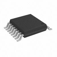
Datasheet Maxim MAX14752EUE+T — 数据表
| 制造商 | Maxim |
| 系列 | MAX14752 |
| 零件号 | MAX14752EUE+T |

8通道/双4通道72 V模拟多路复用器
数据表
MAX14752/MAX14753 8-Channel/Dual 4-Channel 72V Analog Multiplexers General Description
The MAX14752/MAX14753 are 8-to-1 and dual 4-to-1 high-voltage analog multiplexers. Both devices feature 60 (typ) on-resistance with 0.03 (typ) on-resistance flatness. These low on-resistance multiplexers conduct equally well in either direction. Flexible logic levels for the channel-select interface are defined by the EN input. The MAX14752 is a 8-to-1 multiplexer and MAX14753 is a dual 4-to-1 multiplexer. Both devices operate with dual supplies of ±10V to ±36V, or a single supply of +20V to +72V. The MAX14752/MAX14753 are available in a 16-pin TSSOP package and are pin compatible with the industry-standard DG408/DG409. Both the MAX14752/ MAX14753 are specified over the extended -40°C to +85°C operating temperature range. Benefits and Features Supply Range Accommodates Wide Voltage
Applications Wide ±36V (max) Bipolar Power Supply High +72V (max) Single Power Supply Asymmetric Bipolar Power Supply Operation Low Leakage Current and RON Improves System Accuracy Low On-Resistance 60 (typ) 0.03 (typ) RON Flatness Over Common-Mode Voltage Range 20nA Low-Input, On-Leakage Current (max) Low 25µA IDD Supply Current in Disable Mode Saves Power Easy to Upgrade with Pin-Compatible, IndustryStandard DG408/DG409 Applications
Programmable-Logic Controllers Environment Control Systems ATE Systems Medical Monitoring Systems Ordering Information
PART MAX14752EUE+ MAX14753EUE+ TEMP RANGE -40°C to +85°C -40°C to +85°C PIN-PACKAGE 16 TSSOP 16 TSSOP +Denotes a lead(Pb)-free/RoHS-compliant package. Pin Configurations appear at end of data sheet. Functional Diagrams
MAX14752 VDD IN0 IN1 IN2 IN3 OUT IN4 IN5 IN6 IN7 CONTROL INB0 INB1 OUTB INB2 INB3 CONTROL VSS INA0 INA1 INA2 INA3 OUTA VDD MAX14753 VSS S0 S1 S2 EN GND S1 S0 EN GND 19-4255; Rev 5; 5/15 MAX14752/MAX14753 8-Channel/Dual 4-Channel 72V Analog Multiplexers Absolute Maximum Ratings
VDD to VSS .-0.3V to +72V GND to VSS .-0.3V to VDD EN, S0, S1, S2 to GND . .-0.3V to the lesser of (+12V and VDD + 0.3V) IN_, INA_, INB_, OUT, OUTA, OUTB to VSS . .-2V to (VDD -VSS + 2V) or 100mA (whichever occurs first) Continuous Current into IN_, INA_, INB_, OUT, OUTA, OUTB .100mA Continuous Power Dissipation (TA = +70°C) 16-Pin TSSOP (derate 11.1mW/°C above +70°C) .890mW Junction-to-Ambient Thermal Resistance (JA) (Note 1) 16-Pin TSSOP .90°C/W Junction-to-Case Thermal Resistance (JC) (Note 1) 16-Pin TSSOP .27°C/W Maximum Operating Temperature Range .-40°C to +125°C Junction Temperature . +150°C Storage Temperature Range .-65°C to +150°C Lead Temperature …
价格
模型线
- MAX14752EUE+ MAX14752EUE+T MAX14753EUE+ MAX14753EUE+T
制造商分类
- Analog > Switches and Multiplexers