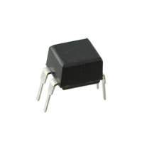
Datasheet Vishay SiHLD024 — 数据表
| 制造商 | Vishay |
| 系列 | SiHLD024 |
| 零件号 | SiHLD024 |

功率MOSFET
数据表
IRLD024, SiHLD024
Vishay Siliconix Power MOSFET
PRODUCT SUMMARY
VDS (V) RDS(on) () Qg (Max.) (nC) Qgs (nC) Qgd (nC) Configuration VGS = 5.0 V 18 4.5 12 Single
D FEATURES
60 0.10 Dynamic dV/dt Rating For Automatic Insertion End Stackable Logic-Level Gate Drive RDS(on) Specified at VGS = 4 V and 5 V 175 °C Operating Temperature Fast Switching Compliant to RoHS Directive 2002/95/EC
Available RoHS*
COMPLIANT HVMDIP DESCRIPTION
G S D G S N-Channel MOSFET Third generation Power MOSFETs from Vishay provide the designer with the best combination of fast switching, ruggedized device design, low on-resistance and cost-effectiveness. The 4 pin DIP package is a low cost machine-insertiable case style which can be stacked in multiple combinations on standard 0.1" pin centers. The dual drain servers as a thermal link to the mounting surface for power dissipation levels up to 1 W. ORDERING INFORMATION
Package Lead (Pb)-free SnPb HVMDIP IRLD024PbF SiHLD024-E3 IRLD024 SiHLD024 ABSOLUTE MAXIMUM RATINGS (TA = 25 °C, unless otherwise noted)
PARAMETER Drain-Source Voltage Gate-Source Voltage Continuous Drain Current Pulsed Drain Currenta VGS at 5.0 V TA = 25 °C TA = 100 °C SYMBOL VDS VGS ID IDM Energyb TA = 25 °C EAS PD dV/dt TJ, Tstg for 10 s LIMIT 60 ± 10 2.5 1.8 20 0.0083 91 1.3 4.5 -55 to + 175 300d W/°C mJ W V/ns °C A UNIT V Linear Derating Factor Single Pulse Avalanche Maximum Power Dissipation Peak Diode Recovery dV/dtc Operating Junction and Storage Temperature Range Soldering Recommendations (Peak Temperature) Notes a. Repetitive rating; pulse width limited by maximum junction temperature (see fig. 11). b. VDD = 25 V, starting TJ = 25 °C, L = 16 mH, Rg = 25 , IAS = 2.5 A (see fig. 12). c. ISD 17 A, dI/dt 140 A/µs, VDD VDS, TJ 175 °C. d. 1.6 mm from case. * Pb containing terminations are not RoHS compliant, exemptions may apply Document Number: 91308 S10-2465-Rev. C, 08-Nov-10 www.vishay.com 1 IRLD024, SiHLD024
Vishay Siliconix
THERMAL RESISTANCE RATINGS
PARAMETER Maximum Junction-to-Ambient SYMBOL RthJA TYP. MAX. 120 UNIT °C/W SPECIFICATIONS (TJ = 25 °C, unless otherwise noted)
PARAMETER Static Drain-Source Breakdown Voltage VDS Temperature Coefficient Gate-Source Threshold Voltage Gate-Source Leakage Zero Gate Voltage Drain Current VDS VDS/TJ VGS(th) IGSS IDSS RDS(on) gfs Ciss Coss Crss Qg Qgs Qgd td(on) tr td(off) tf LD LS Between lead, 6 mm (0.25") from package and center of die contact
D SYMBOL TEST CONDITIONS MIN. TYP. MAX. UNIT VGS = 0 V, ID = 250 µA Reference to 25 °C, ID = 1 mA VDS = VGS, ID = 250 µA VGS = ± 10 V VDS = 60 V, VGS = 0 V VDS = 48 V, VGS = 0 V, …
价格
模型线
- SiHLD024 SiHLD024-E3
制造商分类
- MOSFETs