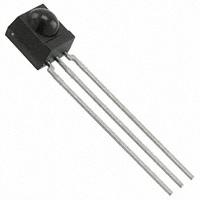
Datasheet Vishay TSSP4P38 — 数据表
| 制造商 | Vishay |
| 系列 | TSSP4P38 |
| 零件号 | TSSP4P38 |

红外中距离传感器
数据表
TSSP4P38
www.vishay.com Vishay Semiconductors IR Mid Range Proximity Sensors
FEATURES Up to 2 m for proximity sensing Uses modulated bursts at 38 kHz 940 nm peak wavelength Photo detector and preamplifier in one package Low supply current 1 2 3
16672 Shielding against EMI Visible light is suppressed by IR filter Insensitive to supply voltage ripple and noise Supply voltage: 2.5 V to 5.5 V Material categorization: for definitions of compliance please see www.vishay.com/doc?99912 MECHANICAL DATA
Pinning 1 = OUT, 2 = GND, 3 = VS DESCRIPTION
The TSSP4P38 is a compact infrared detector module for proximity sensing applications. It receives 38 kHz modulated signals and has a peak sensitivity of 940 nm. The length of the detector's output pulse varies in proportion to the amount of light reflected from the object being detected. APPLICATIONS Object approach detection for activation of displays and user consoles, signaling of alarms, etc. Simple gesture controls Differentiation of car arrival, static, car departure in parking lots Reflective sensors for toilet flush Navigational sensor for robotics PARTS TABLE
Carrier frequency Package Pinning Dimensions (mm) Mounting Application 38 kHz TSSP4P38 Mold 1 = OUT, 2 = GND, 3 = VS 6.0 W x 6.95 H x 5.6 D Leaded Proximity sensors BLOCK DIAGRAM
16833_5 PROXIMITY SENSING
+3V 3 33 k VS 1 Input AGC Band pass Demodulator OUT
Envelope signal 38 kHz IR emitter +3V 2 PIN Control circuit GND Out to C IR detector Rev. 1.6, 01-Jun-15 1 Document Number: 82474 THIS DOCUMENT IS SUBJECT TO CHANGE WITHOUT NOTICE. THE PRODUCTS DESCRIBED HEREIN AND THIS DOCUMENT ARE SUBJECT TO SPECIFIC DISCLAIMERS, SET FORTH AT www.vishay.com/doc?91000 TSSP4P38
www.vishay.com Vishay Semiconductors
TEST CONDITION SYMBOL VS IS VO VS -VO IO Tj Tstg Tamb Tamb 85 °C t 10 s, 1 mm from case Ptot Tsd VALUE -0.3 to +6 5 -0.3 to 5.5 -0.3 to (VS + 0.3) 5 100 -25 to +85 -25 to +85 10 260 UNIT V mA V V mA °C °C °C mW °C ABSOLUTE MAXIMUM RATINGS
PARAMETER Supply voltage (pin 3) Supply current (pin 3) Output voltage (pin 1) Voltage at output to supply Output current (pin 1) Junction temperature Storage temperature range Operating temperature range Power consumption Soldering temperature Note Stresses beyond those listed under "Absolute Maximum Ratings" may cause permanent damage to the device. This is a stress rating only and functional operation of the device at these or any other conditions beyond those indicated in the operational sections of this specification is not implied. Exposure to absolute maximum rating conditions for extended periods may affect the device …