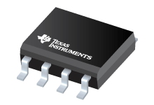
Datasheet Texas Instruments THS4304DBVT — 数据表
| 制造商 | Texas Instruments |
| 系列 | THS4304 |
| 零件号 | THS4304DBVT |

宽带运算放大器5-SOT-23 -40至85
数据表
价格
状态
| Lifecycle Status | Active (Recommended for new designs) |
| Manufacture's Sample Availability | Yes |
打包
| Pin | 5 |
| Package Type | DBV |
| Industry STD Term | SOT-23 |
| JEDEC Code | R-PDSO-G |
| Package QTY | 250 |
| Carrier | SMALL T&R |
| Device Marking | AKW |
| Width (mm) | 1.6 |
| Length (mm) | 2.9 |
| Thickness (mm) | 1.2 |
| Pitch (mm) | .95 |
| Max Height (mm) | 1.45 |
| Mechanical Data | 下载 |
参数化
| 2nd Harmonic | 84 dBc |
| 3rd Harmonic | 100 dBc |
| @ MHz | 10 |
| Acl, min spec gain | 1 V/V |
| Additional Features | N/A |
| Architecture | Bipolar,Voltage FB |
| BW @ Acl | 3000 MHz |
| CMRR(Min) | 80 dB |
| CMRR(Typ) | 95 dB |
| GBW(Typ) | 3000 MHz |
| Input Bias Current(Max) | 12000000 pA |
| Iq per channel(Max) | 18.9 mA |
| Iq per channel(Typ) | 18 mA |
| Number of Channels | 1 |
| Offset Drift(Typ) | 5 uV/C |
| Operating Temperature Range | -40 to 85 C |
| Output Current(Typ) | 100 mA |
| Package Group | SOT-23 |
| Package Size: mm2:W x L | 5SOT-23: 8 mm2: 2.8 x 2.9(SOT-23) PKG |
| Rail-to-Rail | In,Out |
| Rating | Catalog |
| Slew Rate(Typ) | 790 V/us |
| Total Supply Voltage(Max) | 5 +5V=5, +/-5V=10 |
| Total Supply Voltage(Min) | 2.7 +5V=5, +/-5V=10 |
| Vn at 1kHz(Typ) | 6.4 nV/rtHz |
| Vn at Flatband(Typ) | 2.4 nV/rtHz |
| Vos (Offset Voltage @ 25C)(Max) | 4 mV |
生态计划
| RoHS | Compliant |
设计套件和评估模块
- Evaluation Modules & Boards: THS4304DGKEVM
THS4304 Evaluation Module for DGK Package
Lifecycle Status: Active (Recommended for new designs) - Evaluation Modules & Boards: THS4304DBVEVM
THS4304 Evaluation Module for DBV Package
Lifecycle Status: Active (Recommended for new designs)
应用须知
- RF and IF amplifiers with op ampsPDF, 177 Kb, 档案已发布: Feb 28, 2005
- Wideband Complementary Current Output DAC Single-Ended InterfacePDF, 597 Kb, 档案已发布: Jun 21, 2005
High-speed digital-to-analog converters (DACs) most often use a transformer-coupled output stage. In applications where this configuration is not practical, a single op ampdifferential to single-ended stage has often been used. This application note steps through the exact design equations required to achieve gain matching from each output as well as a matched input impedance to each of the DA - Noise Analysis for High Speed Op Amps (Rev. A)PDF, 256 Kb, 修订版: A, 档案已发布: Jan 17, 2005
As system bandwidths have increased an accurate estimate of the noise contribution for each element in the signal channel has become increasingly important. Many designers are not however particularly comfortable with the calculations required to predict the total noise for an op amp or in the conversions between the different descriptions of noise. Considerable inconsistency between manufactu
模型线
系列: THS4304 (9)
制造商分类
- Semiconductors > Amplifiers > Operational Amplifiers (Op Amps) > High-Speed Op Amps (>=50MHz)