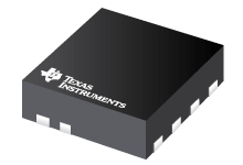
Datasheet Texas Instruments TPS61230ARNSR — 数据表
| 制造商 | Texas Instruments |
| 系列 | TPS61230A |
| 零件号 | TPS61230ARNSR |

采用2.0mm x 2.0mm QFN封装的5V / 6A高效升压转换器7-VQFN-HR -40至125
数据表
TPS61230A 5-V / 6-A High Efficiency Step-Up Converter in 2.0-mm x 2.0-mm VQFN Package datasheet
PDF, 1.3 Mb, 修订版: A, 档案已发布: Aug 24, 2016
从文件中提取
价格
状态
| Lifecycle Status | Active (Recommended for new designs) |
| Manufacture's Sample Availability | Yes |
打包
| Pin | 7 |
| Package Type | RNS |
| Industry STD Term | VQFN-HR |
| JEDEC Code | S-PQFP-N |
| Package QTY | 3000 |
| Carrier | LARGE T&R |
| Device Marking | 12EI |
| Width (mm) | 2 |
| Length (mm) | 2 |
| Thickness (mm) | .9 |
| Pitch (mm) | .5 |
| Max Height (mm) | 1 |
| Mechanical Data | 下载 |
参数化
| Duty Cycle(Max) | 90 % |
| Iq(Typ) | 0.025 mA |
| Operating Temperature Range | -40 to 125 C |
| Package Group | VQFN-HR |
| Rating | Catalog |
| Regulated Outputs | 1 |
| Special Features | Enable,Light Load Efficiency,Load Disconnect,Synchronous Rectification |
| Switch Current Limit(Min) | 4.8 A |
| Switch Current Limit(Typ) | 6 A |
| Switching Frequency(Max) | 1150 kHz |
| Switching Frequency(Min) | 1150 kHz |
| Type | Converter |
| Vin(Max) | 4.5 V |
| Vin(Min) | 2.5 V |
| Vout(Max) | 5.5 V |
| Vout(Min) | 2.5 V |
生态计划
| RoHS | Compliant |
设计套件和评估模块
- Evaluation Modules & Boards: TPS61230AEVM-767
Evaluation Board for TPS61230A 6A High Efficiency Boost Converter in 2-mm Г— 2-mm QFN Package
Lifecycle Status: Active (Recommended for new designs)
应用须知
- Automated Frequency Response AnalyzerPDF, 939 Kb, 档案已发布: Oct 9, 2013
This application report discusses a new method of doing stability Analysis testing by using basic labequipment, while not requiring any specific instruments. - Minimizing Ringing at the Switch Node of a Boost ConverterPDF, 201 Kb, 档案已发布: Sep 15, 2006
The application report explains how to use proper board layout and/or a snubber to reduce high-frequency ringing at the switch node of a boost converter. - Design considerations for a resistive feedback divider in a DC/DC converterPDF, 393 Kb, 档案已发布: Apr 26, 2012
- Basic Calculation of a Boost Converter's Power Stage (Rev. C)PDF, 186 Kb, 修订版: C, 档案已发布: Jan 8, 2014
This application note gives the equations to calculate the power stage of a boost converter built with an IC with integrated switch and operating in continuous conduction mode. It is not intended to give details on the functionality of a boost converter (see Reference 1) or how to compensate a converter. See the references at the end of this document if more detail is needed. - Optimizing Transient Response of Internally Compensated DC-DC Converters (Rev. A)PDF, 1.1 Mb, 修订版: A, 档案已发布: May 11, 2015
- Understanding the Absolute Maximum Ratings of the SW Node (Rev. A)PDF, 755 Kb, 修订版: A, 档案已发布: Jan 13, 2012
- Choosing an Appropriate Pull-up/Pull-down Resistor for Open Drain OutputsPDF, 130 Kb, 档案已发布: Sep 19, 2011
- IQ: What it is what it isn’t and how to use itPDF, 198 Kb, 档案已发布: Jun 17, 2011
- Performing Accurate PFM Mode Efficiency Measurements (Rev. A)PDF, 418 Kb, 修订版: A, 档案已发布: Dec 11, 2018
When performing measurements on DC-DC converters using pulse frequency modulation(PFM)or any power save mode proper care must be taken to ensure that the measurements are accurate. An accurate PFM mode efficiency measurement is critical for systems which require high efficiency at low loads such as in smart home systems tablets wearables and metering.
模型线
系列: TPS61230A (2)
- TPS61230ARNSR TPS61230ARNST
制造商分类
- Semiconductors > Power Management > Non-isolated DC/DC Switching Regulator > Step-Up (Boost) > Boost Converter (Integrated Switch)