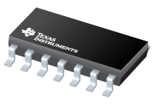
Datasheet Texas Instruments SN74LVC07APWLE — 数据表
| 制造商 | Texas Instruments |
| 系列 | SN74LVC07A |
| 零件号 | SN74LVC07APWLE |

具有漏极开路输出的六路缓冲器/驱动器14-TSSOP -40至85
数据表
SN74LVC07A Hex Buffer and Driver With Open-Drain Outputs datasheet
PDF, 1.2 Mb, 修订版: W, 档案已发布: Nov 13, 2015
从文件中提取
价格
状态
| Lifecycle Status | Obsolete (Manufacturer has discontinued the production of the device) |
| Manufacture's Sample Availability | No |
打包
| Pin | 14 |
| Package Type | PW |
| Industry STD Term | TSSOP |
| JEDEC Code | R-PDSO-G |
| Width (mm) | 4.4 |
| Length (mm) | 5 |
| Thickness (mm) | 1 |
| Pitch (mm) | .65 |
| Max Height (mm) | 1.2 |
| Mechanical Data | 下载 |
参数化
| Approx. Price (US$) | 0.08 | 1ku |
| Bits(#) | 10 |
| F @ Nom Voltage(Max)(Mhz) | 110 |
| ICC @ Nom Voltage(Max)(mA) | 0.01 |
| Input Type | TTL/CMOS |
| Operating Temperature Range(C) | -40 to 125 -40 to 85 |
| Output Drive (IOL/IOH)(Max)(mA) | -24/24 |
| Output Type | LVTTL |
| Package Group | TSSOP |
| Package Size: mm2:W x L (PKG) | 14TSSOP: 32 mm2: 6.4 x 5(TSSOP) |
| Rating | Catalog |
| Schmitt Trigger | No |
| Technology Family | LVC |
| VCC(Max)(V) | 5.5 |
| VCC(Min)(V) | 1.65 |
| Voltage(Nom)(V) | 1.8 2.5 2.7 3.3 5 |
| tpd @ Nom Voltage(Max)(ns) | 5.6 3.4 3.3 3.6 2.6 |
生态计划
| RoHS | Not Compliant |
| Pb Free | No |
应用须知
- LVC07A: Applications Of An Open-Drain Hex Buffer And Discussion Of Char ResultsPDF, 51 Kb, 档案已发布: Apr 8, 1999
The Texas Instruments (TI) LVC07A hex buffer, with open-drain outputs, and its inverting counterpart, LVC06A, operate in the 1.65-V to 3.6-V VCC range, but can accept input voltages up to 5.5 V. Laboratory results show superior propagation times versus competitors, natural Ioff protection, and output-breakdown capability versus a competitor. Applications of the LVC07A and LVC06A include bus-conte - LVC Characterization InformationPDF, 114 Kb, 档案已发布: Dec 1, 1996
This document provides characterization information about low-voltage logic (LVL) that operates from a 3.3-V power supply. It addresses the issues of interfacing to 5-V logic ac performance power considerations input and output characteristics and signal integrity for this family of devices. - Use of the CMOS Unbuffered Inverter in Oscillator CircuitsPDF, 796 Kb, 档案已发布: Nov 6, 2003
CMOS devices have a high input impedance high gain and high bandwidth. These characteristics are similar to ideal amplifier characteristics and hence a CMOS buffer or inverter can be used in an oscillator circuit in conjunction with other passive components. Now CMOS oscillator circuits are widely used in high-speed applications because they are economical easy to use and take significantly
模型线
系列: SN74LVC07A (26)
- SN74LVC07AD SN74LVC07ADBR SN74LVC07ADBRG4 SN74LVC07ADE4 SN74LVC07ADG4 SN74LVC07ADGVR SN74LVC07ADR SN74LVC07ADRE4 SN74LVC07ADRG3 SN74LVC07ADRG4 SN74LVC07ADT SN74LVC07ADTG4 SN74LVC07ANSR SN74LVC07APW SN74LVC07APWE4 SN74LVC07APWG4 SN74LVC07APWLE SN74LVC07APWR SN74LVC07APWRE4 SN74LVC07APWRG3 SN74LVC07APWRG4 SN74LVC07APWT SN74LVC07APWTE4 SN74LVC07APWTG4 SN74LVC07ARGYR SN74LVC07ARGYRG4
制造商分类
- Semiconductors > Logic > Buffer/Driver/Transceiver > Non-Inverting Buffer/Driver