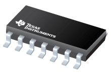
DS14C89A
www.ti.com SNLS081C – MAY 1998 – REVISED APRIL 2013 DS14C89A Quad CMOS Receiver
Check for Samples: DS14C89A FEATURES DESCRIPTION The DS14C89A, pin-for-pin compatible to the
DS1489A/MC1489A, ia a quad receiver designed to
interface data terminal equipment (DTE) with data
circuit-terminating equipment (DCE). These devices
translate levels conforming to EIA-232E and CCITT
V.28 standards to TTL/CMOS logic levels. 1 2 Meets EIA/TIA-232-E and CCITT V.28
Standards
Failsafe -Output High for Open Input
LOW Power Consumption
On Chip Noise Filter
Available in SOIC Package The device is fabricated in low threshold CMOS metal
gate technology. The device provides very low power
consumption compared to their bipolar equivalents:
900 ОјA (DS14C89A) versus 26 mA (DS1489A).
The DS14C89A provides on chip noise filtering which
eliminates the need for external response control filter
capacitors. When replacing the DS1489A with the
DS14C89A, the response control filter pins can be
tied high, low, or not connected. Connection Diagram Figure 1. See Package Number D, NFF0014A 1 2 Please be aware that an important notice concerning availability, standard warranty, and use in critical applications of
Texas Instruments semiconductor products and disclaimers thereto appears at the end of this data sheet.
All trademarks are the property of their respective owners. PRODUCTION DATA information is current as of publication date. …
