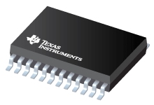
Datasheet Texas Instruments CDC509PWRG4 — 数据表
| 制造商 | Texas Instruments |
| 系列 | CDC509 |
| 零件号 | CDC509PWRG4 |

3.3V锁相环时钟驱动器24-TSSOP 0至70
数据表
价格
状态
| Lifecycle Status | Active (Recommended for new designs) |
| Manufacture's Sample Availability | Yes |
打包
| Pin | 24 |
| Package Type | PW |
| Industry STD Term | TSSOP |
| JEDEC Code | R-PDSO-G |
| Package QTY | 2000 |
| Carrier | LARGE T&R |
| Device Marking | CK509 |
| Width (mm) | 4.4 |
| Length (mm) | 7.8 |
| Thickness (mm) | 1 |
| Pitch (mm) | .65 |
| Max Height (mm) | 1.2 |
| Mechanical Data | 下载 |
参数化
| Absolute Jitter (Peak-to-Peak Cycle or Period Jitter) | 200 ps |
| Number of Outputs | 9 |
| Operating Frequency Range(Max) | 125 MHz |
| Operating Frequency Range(Min) | 25 MHz |
| Operating Temperature Range | 0 to 70 C |
| Package Group | TSSOP |
| Package Size: mm2:W x L | 24TSSOP: 50 mm2: 6.4 x 7.8(TSSOP) PKG |
| Rating | Catalog |
| VCC | 3.3 V |
| t(phase error) | 480 ps |
| tsk(o) | 200 ps |
生态计划
| RoHS | Compliant |
应用须知
- High Speed Clock Distribution Design Techniques for CDC 509/516/2509/2510/2516 (Rev. A)PDF, 109 Kb, 修订版: A, 档案已发布: Sep 23, 1998
The memory bandwidth of high performance microprocessors is increasing at a rapid rate and the future memory bandwidth requirements are expected to keep increasing. The bandwidth requirements of RAM will be satisfied in the near term by using Synchronous DRAM. The need to drive multiple DRAM chips at high speeds with low skew necessitates the use of clock distribution devices with Phase Locked Loo
模型线
制造商分类
- Semiconductors > Clock and Timing > Clock Buffers > Zero Delay Buffers