Datasheet Texas Instruments CDCE913 — 数据表
| 制造商 | Texas Instruments |
| 系列 | CDCE913 |
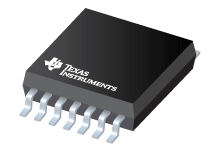
具有2.5V或3.3V LVCMOS输出的可编程1-PLL VCXO时钟合成器
数据表
CDCE(L)913: Flexible Low Power LVCMOS Clock Generator With SSC Support for EMI Reduction datasheet
PDF, 1.8 Mb, 修订版: G, 档案已发布: Oct 27, 2016
从文件中提取
价格
状态
| CDCE913PW | CDCE913PWG4 | CDCE913PWR | CDCE913PWRG4 | |
|---|---|---|---|---|
| Lifecycle Status | Active (Recommended for new designs) | Active (Recommended for new designs) | Active (Recommended for new designs) | Active (Recommended for new designs) |
| Manufacture's Sample Availability | No | No | Yes | Yes |
打包
| CDCE913PW | CDCE913PWG4 | CDCE913PWR | CDCE913PWRG4 | |
|---|---|---|---|---|
| N | 1 | 2 | 3 | 4 |
| Pin | 14 | 14 | 14 | 14 |
| Package Type | PW | PW | PW | PW |
| Industry STD Term | TSSOP | TSSOP | TSSOP | TSSOP |
| JEDEC Code | R-PDSO-G | R-PDSO-G | R-PDSO-G | R-PDSO-G |
| Package QTY | 90 | 90 | 2000 | 2000 |
| Carrier | TUBE | TUBE | LARGE T&R | LARGE T&R |
| Device Marking | CDCE913 | CDCE913 | CDCE913 | CDCE913 |
| Width (mm) | 4.4 | 4.4 | 4.4 | 4.4 |
| Length (mm) | 5 | 5 | 5 | 5 |
| Thickness (mm) | 1 | 1 | 1 | 1 |
| Pitch (mm) | .65 | .65 | .65 | .65 |
| Max Height (mm) | 1.2 | 1.2 | 1.2 | 1.2 |
| Mechanical Data | 下载 | 下载 | 下载 | 下载 |
参数化
| Parameters / Models | CDCE913PW | CDCE913PWG4 | CDCE913PWR | CDCE913PWRG4 |
|---|---|---|---|---|
| Input Level | Crystal,LVCMOS | Crystal,LVCMOS | Crystal,LVCMOS | Crystal,LVCMOS |
| Number of Outputs | 3 | 3 | 3 | 3 |
| Operating Temperature Range, C | -40 to 85 | -40 to 85 | -40 to 85 | -40 to 85 |
| Output Frequency(Max), MHz | 230 | 230 | 230 | 230 |
| Output Level | LVCMOS | LVCMOS | LVCMOS | LVCMOS |
| Package Group | TSSOP | TSSOP | TSSOP | TSSOP |
| Package Size: mm2:W x L, PKG | 14TSSOP: 32 mm2: 6.4 x 5(TSSOP) | 14TSSOP: 32 mm2: 6.4 x 5(TSSOP) | 14TSSOP: 32 mm2: 6.4 x 5(TSSOP) | 14TSSOP: 32 mm2: 6.4 x 5(TSSOP) |
| Programmability | EEPROM | EEPROM | EEPROM | EEPROM |
| Special Features | Integrated EEPROM,I2C,Pin Programming,Spread Spectrum Clocking (SSC) | Integrated EEPROM,I2C,Pin Programming,Spread Spectrum Clocking (SSC) | Integrated EEPROM,I2C,Pin Programming,Spread Spectrum Clocking (SSC) | Integrated EEPROM,I2C,Pin Programming,Spread Spectrum Clocking (SSC) |
| VCC Core, V | 1.8 | 1.8 | 1.8 | 1.8 |
| VCC Out, V | 2.5,3.3 | 2.5,3.3 | 2.5,3.3 | 2.5,3.3 |
生态计划
| CDCE913PW | CDCE913PWG4 | CDCE913PWR | CDCE913PWRG4 | |
|---|---|---|---|---|
| RoHS | Compliant | Compliant | Compliant | Compliant |
应用须知
- General I2C / EEPROM usage for the CDCE(L)9xx familyPDF, 40 Kb, 档案已发布: Jan 26, 2010
- VCXO Application Guideline for CDCE(L)9xx Family (Rev. A)PDF, 107 Kb, 修订版: A, 档案已发布: Apr 23, 2012
- Practical consideration on choosing a crystal for CDCE(L)9xx familyPDF, 60 Kb, 档案已发布: Mar 24, 2008
- Usage of I2C for CDCE(L)949, CDCE(L)937, CDCE(L)925, CDCE(L)913PDF, 297 Kb, 档案已发布: Sep 23, 2009
This document presents a method to smoothly change frequency by IВІCв„ў protocol on Texas Instruments CDCE(L)949, CDCE(L)937, CDCE(L)925, CDCE(L)913 Clock Synthesizers, thus avoiding unnecessary intermediate frequencies. It also includes a code example to generate the IВІC protocol for the CDCE(L)9xx with the TMS320C645x. - Generating Low Phase-Noise Clocks for Audio Data Converters from Low FrequencyPDF, 860 Kb, 档案已发布: Mar 31, 2008
Generating a high-frequency system clock Fs (128fs to 768fs) from a low-frequency sampling clock fs (10 kHz to 200 kHz) is challenging, while attempting to maintain low phase jitter. A traditional phase-lock loop (PLL) can do the frequency translation, but the added phase jitter prevents the generated system clock signal from effectively driving high-performance audio data converters. This applica - Troubleshooting I2C Bus ProtocolPDF, 184 Kb, 档案已发布: Oct 19, 2009
When using the I2Cв„ў bus protocol, the designer must ensure that the hardware complies with the I2C standard. This application report describes the I2C protocol and provides guidelines on debugging a missing acknowledgment, selecting the pullup resistors, or meeting the maximum capacitance load of an I2C bus. A conflict occurs if devices sharing the I2C bus have the same slave address. This
模型线
系列: CDCE913 (4)
制造商分类
- Semiconductors> Clock and Timing> Clock Generators> General Purpose