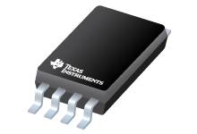
Datasheet Texas Instruments CDCLVC1103PW — 数据表
| 制造商 | Texas Instruments |
| 系列 | CDCLVC1103 |
| 零件号 | CDCLVC1103PW |

低抖动,1:3 LVCMOS扇出时钟缓冲器8-TSSOP -40至85
数据表
CDCLVC11xx 3.3-V and 2.5-V LVCMOS High-Performance Clock Buffer Family datasheet
PDF, 1.6 Mb, 修订版: B, 档案已发布: Feb 24, 2017
从文件中提取
价格
状态
| Lifecycle Status | Active (Recommended for new designs) |
| Manufacture's Sample Availability | No |
打包
| Pin | 8 |
| Package Type | PW |
| Industry STD Term | TSSOP |
| JEDEC Code | R-PDSO-G |
| Package QTY | 150 |
| Carrier | TUBE |
| Device Marking | C9C3 |
| Width (mm) | 4.4 |
| Length (mm) | 3 |
| Thickness (mm) | 1 |
| Pitch (mm) | .65 |
| Max Height (mm) | 1.2 |
| Mechanical Data | 下载 |
参数化
| Additive RMS Jitter(Typ) | 70 fs |
| Input Frequency(Max) | 250 MHz |
| Input Level | LVCMOS |
| Number of Outputs | 3 |
| Operating Temperature Range | -40 to 85 C |
| Output Frequency(Max) | 250 MHz |
| Output Level | LVCMOS |
| Package Group | TSSOP |
| Package Size: mm2:W x L | 8TSSOP: 19 mm2: 6.4 x 3(TSSOP) PKG |
| Rating | Catalog |
| VCC Out | 2.5,3.3 V |
生态计划
| RoHS | Compliant |
设计套件和评估模块
- Evaluation Modules & Boards: CDCLVC1104EVM
CDCLVC1104 Evaluation Module
Lifecycle Status: Active (Recommended for new designs) - Evaluation Modules & Boards: DLPLCR9000EVM
DLPВ® LightCrafterВ™ 9000 Evaluation Module
Lifecycle Status: Active (Recommended for new designs)
应用须知
- How to Apply 1.8-V Signals to 3.3-V CDCLVC11xx Fanout Clock BufferPDF, 518 Kb, 档案已发布: Nov 30, 2010
The CDCLVC11xx buffer family from Texas Instruments has a nominal voltage supply of 2.5 V and 3.3 V. With the simple employment of an external RC network, this family of devices can handle incoming signals whose voltage levels go up to 1.8 V. This application report explains how to implement this network and dimension its discrete components, without impacting the specifications of additive ji
模型线
系列: CDCLVC1103 (2)
- CDCLVC1103PW CDCLVC1103PWR
制造商分类
- Semiconductors > Clock and Timing > Clock Buffers > Single-Ended