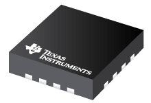
CDCLVD2102
www.ti.com SCAS904A – MAY 2010 – REVISED JUNE 2010 Dual 1:2 Low Additive Jitter LVDS Buffer
Check for Samples: CDCLVD2102 FEATURES 1 Dual 1:2 Differential Buffer
Low Additive Jitter 3000 V Stresses beyond those listed under “absolute maximum ratings” may cause permanent damage to the device. These are stress ratings
only and functional operation of the device at these or any other conditions beyond those indicated under recommended operating
conditions” is not implied. Exposure to absolute–maximum–rated conditions for extended periods may affect device reliability.
The outputs can handle permanent short. RECOMMENDED OPERATING CONDITIONS
Device supply voltage, VCC
Ambient temperature, TA MIN TYP MAX 2.375 2.5 2.625 –40 85 UNITS
V
oC Submit Documentation Feedback Copyright В© 2010, Texas Instruments Incorporated Product Folder Link(s): CDCLVD2102 3 CDCLVD2102
SCAS904A – MAY 2010 – REVISED JUNE 2010 www.ti.com THERMAL INFORMATION
CDCLVD2102
THERMAL METRIC (1) RGT UNITS 16 PINS
qJA Junction-to-ambient thermal resistance 51.3 qJC(top) Junction-to-case(top) thermal resistance 85.4 qJB Junction-to-board thermal resistance 20.1 yJT Junction-to-top characterization parameter 1.3 yJB Junction-to-board characterization parameter 19.4 qJC(bottom) Junction-to-case(bottom) thermal resistance 6 (1) В°C/W For more information about traditional and new thermal metrics, see the IC Package Thermal Metrics application report, SPRA953. ELECTRICAL CHARACTERISTICS:
At VCC = 2.375 V to 2.625 V and TA = –40°C to 85°C (unless otherwise noted).
PARAMETER TEST CONDITIONS MIN TYP MAX UNIT EN PIN INPUT CHARACTERISTICS
VdI3 3-State VdIH Input high voltage Open VdIL Input low voltage IdIH Input high current VCC = 2.625 V, VIH = 2.625 V IdIL Input low current VCC = 2.625 V, VIL = 0 V Rpull(EN) Input pull-up/ pull-down resistor 0.5Г—VCC V 0.7Г—VCC V
0.2×VCC V 30 mA –30 mA 200 kΩ 2.5V LVCMOS (see Figure 7) INPUT CHARACTERISTICS
fIN Input frequency
External threshold voltage applied
to complementary input Vth Input threshold voltage VIH Input high voltage VIL Input low voltage IIH Input high current VCC = 2.625 V, VIH = 2.625 V IIL Input low current VCC = 2.625 V, VIL = 0 V ΔV/ΔT Input edge rate 20% – 80% CIN Input capacitance 200 MHz 1.5 V Vth + 0.1 VCC V 0 Vth – 0.1 V 10 mA 1.1 –10
1.5 mA …


