Sample &
Buy Product
Folder Support &
Community Tools &
Software Technical
Documents CSD19534Q5A
SLPS483 – MAY 2014 CSD19534Q5A 100 V N-Channel NexFET™ Power MOSFETs
1 Features Product Summary Ultra-Low Qg and Qgd
Low Thermal Resistance
Avalanche Rated
Pb-Free Terminal Plating
RoHS Compliant
Halogen Free
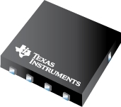
SON 5 mm Г— 6 mm Plastic Package 1 TA = 25В°C TYPICAL VALUE Drain-to-Source Voltage 100 V Qg Gate Charge Total (10 V) 17 nC Qgd Gate Charge Gate to Drain 3.2 RDS(on) Drain-to-Source On Resistance VGS(th) Threshold Voltage Primary Side Telecom
Motor Control 3 Description
This 100 V, 12.6 mО©, SON 5 mm x 6mm NexFETв„ў
power MOSFET is designed to minimize losses in
power conversion applications. 14.1 mΩ VGS = 10 V 12.6 mΩ 2.8 Top View S Device Media Qty Package Ship 13-Inch Reel 2500 CSD19534Q5AT 7-Inch Reel 250 SON 5 x 6 mm
Plastic Package Tape and
Reel (1) For all available packages, see the orderable addendum at
the end of the data sheet. Absolute Maximum Ratings 8 1 7 2 D D VALUE UNIT VDS Drain-to-Source Voltage 100 V VGS Gate-to-Source Voltage В±20 V Continuous Drain Current (Package limited) 50 Continuous Drain Current (Silicon limited),
TC = 25В°C 44 ID (1) S 6 3 D IDM D
G V CSD19534Q5A TA = 25В°C S nC VGS = 6 V . …


