Datasheet Texas Instruments LMR10510 — 数据表
| 制造商 | Texas Instruments |
| 系列 | LMR10510 |
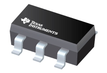
采用SOT-23封装的3V至5.5V,1A降压型DC / DC开关稳压器
数据表
SIMPLE SWITCHER 5.5Vin, 1A Step-Down Voltage Regulator in SOT-23 and LLP datasheet
PDF, 1.1 Mb, 修订版: B, 档案已发布: Apr 4, 2013
从文件中提取
价格
状态
| LMR10510XMF/NOPB | LMR10510XMFE/NOPB | LMR10510XMFX/NOPB | LMR10510YMF/NOPB | LMR10510YMFE/NOPB | LMR10510YMFX/NOPB | LMR10510YSD/NOPB | LMR10510YSDE/NOPB | LMR10510YSDX/NOPB | |
|---|---|---|---|---|---|---|---|---|---|
| Lifecycle Status | Active (Recommended for new designs) | Active (Recommended for new designs) | Active (Recommended for new designs) | Active (Recommended for new designs) | Active (Recommended for new designs) | Active (Recommended for new designs) | Active (Recommended for new designs) | Active (Recommended for new designs) | Active (Recommended for new designs) |
| Manufacture's Sample Availability | Yes | Yes | No | Yes | No | No | Yes | Yes | Yes |
打包
| LMR10510XMF/NOPB | LMR10510XMFE/NOPB | LMR10510XMFX/NOPB | LMR10510YMF/NOPB | LMR10510YMFE/NOPB | LMR10510YMFX/NOPB | LMR10510YSD/NOPB | LMR10510YSDE/NOPB | LMR10510YSDX/NOPB | |
|---|---|---|---|---|---|---|---|---|---|
| N | 1 | 2 | 3 | 4 | 5 | 6 | 7 | 8 | 9 |
| Pin | 5 | 5 | 5 | 5 | 5 | 5 | 6 | 6 | 6 |
| Package Type | DBV | DBV | DBV | DBV | DBV | DBV | NGG | NGG | NGG |
| Industry STD Term | SOT-23 | SOT-23 | SOT-23 | SOT-23 | SOT-23 | SOT-23 | WSON | WSON | WSON |
| JEDEC Code | R-PDSO-G | R-PDSO-G | R-PDSO-G | R-PDSO-G | R-PDSO-G | R-PDSO-G | S-PDSO-N | S-PDSO-N | S-PDSO-N |
| Package QTY | 1000 | 250 | 3000 | 1000 | 250 | 3000 | 1000 | 250 | 4500 |
| Carrier | LARGE T&R | SMALL T&R | LARGE T&R | LARGE T&R | SMALL T&R | LARGE T&R | SMALL T&R | SMALL T&R | LARGE T&R |
| Device Marking | SH7B | SH7B | SH7B | SH9B | SH9B | SH9B | L268B | L268B | L268B |
| Width (mm) | 1.6 | 1.6 | 1.6 | 1.6 | 1.6 | 1.6 | 3 | 3 | 3 |
| Length (mm) | 2.9 | 2.9 | 2.9 | 2.9 | 2.9 | 2.9 | 3 | 3 | 3 |
| Thickness (mm) | 1.2 | 1.2 | 1.2 | 1.2 | 1.2 | 1.2 | .8 | .8 | .8 |
| Pitch (mm) | .95 | .95 | .95 | .95 | .95 | .95 | .95 | .95 | .95 |
| Max Height (mm) | 1.45 | 1.45 | 1.45 | 1.45 | 1.45 | 1.45 | .8 | .8 | .8 |
| Mechanical Data | 下载 | 下载 | 下载 | 下载 | 下载 | 下载 | 下载 | 下载 | 下载 |
参数化
| Parameters / Models | LMR10510XMF/NOPB | LMR10510XMFE/NOPB | LMR10510XMFX/NOPB | LMR10510YMF/NOPB | LMR10510YMFE/NOPB | LMR10510YMFX/NOPB | LMR10510YSD/NOPB | LMR10510YSDE/NOPB | LMR10510YSDX/NOPB |
|---|---|---|---|---|---|---|---|---|---|
| Control Mode | Current Mode | Current Mode | Current Mode | Current Mode | Current Mode | Current Mode | Current Mode | Current Mode | Current Mode |
| Duty Cycle(Max), % | 94 | 94 | 94 | 94 | 94 | 94 | 94 | 94 | 94 |
| Iout(Max), A | 1 | 1 | 1 | 1 | 1 | 1 | 1 | 1 | 1 |
| Iq(Typ), mA | 3.3 | 3.3 | 3.3 | 3.3 | 3.3 | 3.3 | 3.3 | 3.3 | 3.3 |
| Operating Temperature Range, C | -40 to 125 | -40 to 125 | -40 to 125 | -40 to 125 | -40 to 125 | -40 to 125 | -40 to 125 | -40 to 125 | -40 to 125 |
| Package Group | SOT-23 | SOT-23 | SOT-23 | SOT-23 | SOT-23 | SOT-23 | WSON | WSON | WSON |
| Rating | Catalog | Catalog | Catalog | Catalog | Catalog | Catalog | Catalog | Catalog | Catalog |
| Regulated Outputs | 1 | 1 | 1 | 1 | 1 | 1 | 1 | 1 | 1 |
| Special Features | Enable | Enable | Enable | Enable | Enable | Enable | Enable | Enable | Enable |
| Switching Frequency(Max), kHz | 3000 | 3000 | 3000 | 3000 | 3000 | 3000 | 3000 | 3000 | 3000 |
| Switching Frequency(Min), kHz | 1600 | 1600 | 1600 | 1600 | 1600 | 1600 | 1600 | 1600 | 1600 |
| Type | Converter | Converter | Converter | Converter | Converter | Converter | Converter | Converter | Converter |
| Vin(Max), V | 5.5 | 5.5 | 5.5 | 5.5 | 5.5 | 5.5 | 5.5 | 5.5 | 5.5 |
| Vin(Min), V | 3 | 3 | 3 | 3 | 3 | 3 | 3 | 3 | 3 |
| Vout(Max), V | 4.5 | 4.5 | 4.5 | 4.5 | 4.5 | 4.5 | 4.5 | 4.5 | 4.5 |
| Vout(Min), V | 0.6 | 0.6 | 0.6 | 0.6 | 0.6 | 0.6 | 0.6 | 0.6 | 0.6 |
生态计划
| LMR10510XMF/NOPB | LMR10510XMFE/NOPB | LMR10510XMFX/NOPB | LMR10510YMF/NOPB | LMR10510YMFE/NOPB | LMR10510YMFX/NOPB | LMR10510YSD/NOPB | LMR10510YSDE/NOPB | LMR10510YSDX/NOPB | |
|---|---|---|---|---|---|---|---|---|---|
| RoHS | Compliant | Compliant | Compliant | Compliant | Compliant | Compliant | Compliant | Compliant | Compliant |
应用须知
- QFN and SON PCB Attachment (Rev. B)PDF, 821 Kb, 修订版: B, 档案已发布: Aug 24, 2018
- AN-643 EMI/RFI Board Design (Rev. B)PDF, 742 Kb, 修订版: B, 档案已发布: May 3, 2004
Application Note 643 EMI/RFI Board Design - Input and Output Capacitor SelectionPDF, 219 Kb, 档案已发布: Sep 19, 2005
- AN-1197 Selecting Inductors for Buck Converters (Rev. B)PDF, 558 Kb, 修订版: B, 档案已发布: Apr 23, 2013
This application report provides design information to help select an off-the-shelf inductor for anycontinuous-mode buck converter application. - AN-2155 Layout Tips for EMI Reduction in DC/ DC Converters (Rev. A)PDF, 3.6 Mb, 修订版: A, 档案已发布: Apr 23, 2013
This application note will explore how the layout of your DC/DC power supply can significantly affect theamount of EMI that it produces. It will discuss several variations of a layout analyze the results andprovide answers to some common EMI questions such whether or not to use a shielded inductor. - AN-1566 Techniques for Thermal Analysis of Switching Power Supply Designs (Rev. A)PDF, 1.4 Mb, 修订版: A, 档案已发布: Apr 23, 2013
This application note provides thermal power analysis techniques for analyzing the power IC. - AN-1889 How to Measure the Loop Transfer Function of Power Supplies (Rev. A)PDF, 2.7 Mb, 修订版: A, 档案已发布: Apr 23, 2013
This application report shows how to measure the critical points of a bode plot with only an audiogenerator (or simple signal generator) and an oscilloscope. The method is explained in an easy to followstep-by-step manner so that a power supply designer can start performing these measurements in a shortamount of time. - Semiconductor and IC Package Thermal Metrics (Rev. C)PDF, 201 Kb, 修订版: C, 档案已发布: Apr 19, 2016
- Absolute Maximum Ratings for Soldering (Rev. D)PDF, 52 Kb, 修订版: D, 档案已发布: Jun 9, 2016
- AN-1149 Layout Guidelines for Switching Power Supplies (Rev. C)PDF, 82 Kb, 修订版: C, 档案已发布: Apr 23, 2013
When designing a high frequency switching regulated power supply layout is very important. Using agood layout can solve many problems associated with these types of supplies. The problems due to a badlayout are often seen at high current levels and are usually more obvious at large input to output voltagedifferentials. Some of the main problems are loss of regulation at high output current - AN-1229 SIMPLE SWITCHER PCB Layout Guidelines (Rev. C)PDF, 374 Kb, 修订版: C, 档案已发布: Apr 23, 2013
This application report provides SIMPLE SWITCHER™ PCB layout guidelines. - AN-2162 Simple Success With Conducted EMI From DC-DC Converters (Rev. C)PDF, 2.5 Mb, 修订版: C, 档案已发布: Apr 24, 2013
Electromagnetic Interference (EMI) is an unwanted effect between two electrical systems as a result ofeither electromagnetic radiation or electromagnetic conduction. EMI is the major adverse effect caused bythe application of switch-mode power supplies (SMPS). In switching power supplies EMI noise isunavoidable due to the switching actions of the semiconductor devices and resulting disconti - AN-1246 Stresses in Wide Input DC-DC Converters (Rev. C)PDF, 427 Kb, 修订版: C, 档案已发布: Apr 23, 2013
This application note discusses stresses in wide input DC-DC converters. - AN-1520 A Guide to Board Layout for Best Thermal Resistance for Exposed Packages (Rev. B)PDF, 9.2 Mb, 修订版: B, 档案已发布: Apr 23, 2013
This thermal application report provides guidelines for the optimal board layout to achieve the best thermalresistance for exposed packages. The thermal resistance between junction-to-ambient (ОёJA) is highlydependent on the PCB (Printed Circuit Board) design factors. This becomes more critical for packageshaving very low thermal resistance between junction-to-case such as exposed pad TSSOP
模型线
系列: LMR10510 (9)
制造商分类
- Semiconductors> Power Management> Non-isolated DC/DC Switching Regulator> Step-Down (Buck)> Buck Converter (Integrated Switch)