Datasheet Texas Instruments OPA2613 — 数据表
| 制造商 | Texas Instruments |
| 系列 | OPA2613 |
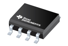
具有电流限制的双宽带,高输出电流,运算放大器
数据表
Dual, Wideband, High Output Current, Operational Amplifier with Current Limit datasheet
PDF, 709 Kb, 修订版: H, 档案已发布: Aug 28, 2008
从文件中提取
价格
状态
| OPA2613ID | OPA2613IDR | OPA2613IDRG4 | OPA2613IDTJ | OPA2613IDTJG3 | OPA2613IDTJR | OPA2613IDTJRG3 | |
|---|---|---|---|---|---|---|---|
| Lifecycle Status | Active (Recommended for new designs) | Active (Recommended for new designs) | Active (Recommended for new designs) | Obsolete (Manufacturer has discontinued the production of the device) | Obsolete (Manufacturer has discontinued the production of the device) | Obsolete (Manufacturer has discontinued the production of the device) | Obsolete (Manufacturer has discontinued the production of the device) |
| Manufacture's Sample Availability | No | No | No | No | No | No | No |
打包
| OPA2613ID | OPA2613IDR | OPA2613IDRG4 | OPA2613IDTJ | OPA2613IDTJG3 | OPA2613IDTJR | OPA2613IDTJRG3 | |
|---|---|---|---|---|---|---|---|
| N | 1 | 2 | 3 | 4 | 5 | 6 | 7 |
| Pin | 8 | 8 | 8 | 8 | 8 | 8 | 8 |
| Package Type | D | D | D | DTJ | DTJ | DTJ | DTJ |
| Industry STD Term | SOIC | SOIC | SOIC | HSOIC | HSOIC | HSOIC | HSOIC |
| JEDEC Code | R-PDSO-G | R-PDSO-G | R-PDSO-G | R-PDSO-G | R-PDSO-G | R-PDSO-G | R-PDSO-G |
| Package QTY | 75 | 2500 | 2500 | ||||
| Carrier | TUBE | LARGE T&R | LARGE T&R | ||||
| Device Marking | 2613 | OPA | OPA | ||||
| Width (mm) | 3.91 | 3.91 | 3.91 | 3.9 | 3.9 | 3.9 | 3.9 |
| Length (mm) | 4.9 | 4.9 | 4.9 | 4.89 | 4.89 | 4.89 | 4.89 |
| Thickness (mm) | 1.58 | 1.58 | 1.58 | 1.39 | 1.39 | 1.39 | 1.39 |
| Pitch (mm) | 1.27 | 1.27 | 1.27 | 1.27 | 1.27 | 1.27 | 1.27 |
| Max Height (mm) | 1.75 | 1.75 | 1.75 | 1.75 | 1.75 | 1.75 | 1.75 |
| Mechanical Data | 下载 | 下载 | 下载 | 下载 | 下载 | 下载 | 下载 |
参数化
| Parameters / Models | OPA2613ID | OPA2613IDR | OPA2613IDRG4 | OPA2613IDTJ | OPA2613IDTJG3 | OPA2613IDTJR | OPA2613IDTJRG3 |
|---|---|---|---|---|---|---|---|
| 2nd Harmonic, dBc | 70 | 70 | 70 | ||||
| 2nd Harmonic(dBc) | 70 | 70 | 70 | 70 | |||
| 3rd Harmonic, dBc | 84 | 84 | 84 | ||||
| 3rd Harmonic(dBc) | 84 | 84 | 84 | 84 | |||
| @ MHz | 1 | 1 | 1 | 1 | 1 | 1 | 1 |
| Acl, min spec gain, V/V | 1 | 1 | 1 | ||||
| Acl, min spec gain(V/V) | 1 | 1 | 1 | 1 | |||
| Additional Features | N/A | N/A | N/A | N/A | N/A | N/A | N/A |
| Approx. Price (US$) | 1.70 | 1ku | 1.70 | 1ku | 1.70 | 1ku | 1.70 | 1ku | |||
| Architecture | Bipolar,Voltage FB | Bipolar,Voltage FB | Bipolar,Voltage FB | Bipolar Voltage FB | Bipolar Voltage FB | Bipolar Voltage FB | Bipolar Voltage FB |
| BW @ Acl, MHz | 230 | 230 | 230 | ||||
| BW @ Acl(MHz) | 230 | 230 | 230 | 230 | |||
| CMRR(Min), dB | 88 | 88 | 88 | ||||
| CMRR(Min)(dB) | 88 | 88 | 88 | 88 | |||
| CMRR(Typ), dB | 100 | 100 | 100 | ||||
| CMRR(Typ)(dB) | 100 | 100 | 100 | 100 | |||
| GBW(Typ), MHz | 230 | 230 | 230 | ||||
| GBW(Typ)(MHz) | 230 | 230 | 230 | 230 | |||
| Input Bias Current(Max), pA | 12000 | 12000 | 12000 | ||||
| Input Bias Current(Max)(pA) | 12000 | 12000 | 12000 | 12000 | |||
| Iq per channel(Max), mA | 6.2 | 6.2 | 6.2 | ||||
| Iq per channel(Max)(mA) | 6.2 | 6.2 | 6.2 | 6.2 | |||
| Iq per channel(Typ), mA | 6 | 6 | 6 | ||||
| Iq per channel(Typ)(mA) | 6 | 6 | 6 | 6 | |||
| Number of Channels | 2 | 2 | 2 | ||||
| Number of Channels(#) | 2 | 2 | 2 | 2 | |||
| Offset Drift(Typ), uV/C | 3.3 | 3.3 | 3.3 | ||||
| Offset Drift(Typ)(uV/C) | 3.3 | 3.3 | 3.3 | 3.3 | |||
| Operating Temperature Range, C | -40 to 85 | -40 to 85 | -40 to 85 | ||||
| Operating Temperature Range(C) | -40 to 85 | -40 to 85 | -40 to 85 | -40 to 85 | |||
| Output Current(Typ), mA | 350 | 350 | 350 | ||||
| Output Current(Typ)(mA) | 350 | 350 | 350 | 350 | |||
| Package Group | SOIC | SOIC | SOIC | SOIC | SOIC | SOIC | SOIC |
| Package Size: mm2:W x L, PKG | 8SOIC: 29 mm2: 6 x 4.9(SOIC) | 8SOIC: 29 mm2: 6 x 4.9(SOIC) | 8SOIC: 29 mm2: 6 x 4.9(SOIC) | ||||
| Package Size: mm2:W x L (PKG) | 8SOIC: 29 mm2: 6 x 4.9(SOIC) | 8SOIC: 29 mm2: 6 x 4.9(SOIC) | 8SOIC: 29 mm2: 6 x 4.9(SOIC) | 8SOIC: 29 mm2: 6 x 4.9(SOIC) | |||
| Rail-to-Rail | No | No | No | No | No | No | No |
| Rating | Catalog | Catalog | Catalog | Catalog | Catalog | Catalog | Catalog |
| Slew Rate(Typ), V/us | 60 | 60 | 60 | ||||
| Slew Rate(Typ)(V/us) | 60 | 60 | 60 | 60 | |||
| Total Supply Voltage(Max), +5V=5, +/-5V=10 | 12 | 12 | 12 | ||||
| Total Supply Voltage(Max)(+5V=5, +/-5V=10) | 12 | 12 | 12 | 12 | |||
| Total Supply Voltage(Min), +5V=5, +/-5V=10 | 5 | 5 | 5 | ||||
| Total Supply Voltage(Min)(+5V=5, +/-5V=10) | 5 | 5 | 5 | 5 | |||
| Vn at 1kHz(Typ), nV/rtHz | 1.9 | 1.9 | 1.9 | ||||
| Vn at Flatband(Typ), nV/rtHz | 1.8 | 1.8 | 1.8 | ||||
| Vn at Flatband(Typ)(nV/rtHz) | 1.8 | 1.8 | 1.8 | 1.8 | |||
| Vos (Offset Voltage @ 25C)(Max), mV | 1 | 1 | 1 | ||||
| Vos (Offset Voltage @ 25C)(Max)(mV) | 1 | 1 | 1 | 1 |
生态计划
| OPA2613ID | OPA2613IDR | OPA2613IDRG4 | OPA2613IDTJ | OPA2613IDTJG3 | OPA2613IDTJR | OPA2613IDTJRG3 | |
|---|---|---|---|---|---|---|---|
| RoHS | Compliant | Compliant | Compliant | Not Compliant | Not Compliant | Not Compliant | Not Compliant |
| Pb Free | No | No | No | No |
应用须知
- Active Output Impedance for ADSL Line DriversPDF, 636 Kb, 档案已发布: Nov 26, 2002
Signal termination is very common in bidirectional communication systems. Termination allows for receiving signals while transmitting different signals at the same time. With the increasing popularity of asymmetrical digital subscriber lines (ADSL), the requirement for a low power line driver amplifier combined with line termination becomes a very difficult goal. This application note examines the - RLC Filter Design for ADC Interface Applications (Rev. A)PDF, 299 Kb, 修订版: A, 档案已发布: May 13, 2015
As high performance Analog-to-Digital Converters (ADCs) continue to improve in their performance, the last stage interface from the final amplifier into the converter inputs becomes a critical element in the system design if the full converter dynamic range is desired. This application note describes the performance and design equations for a simple passive 2nd-order filter used successfully in AD - ADS5500, OPA695: PC Board Layout for Low Distortion High-Speed ADC DriversPDF, 273 Kb, 档案已发布: Apr 22, 2004
Once an analog-to-digital converter (ADC) and a driver/interface have been selected for a given application, the next step to achieving excellent performance is laying out the printed circuit board (PCB) that will support the application. This application report describes several techniques for optimizing a high-speed, 14-bit performance, differential driver PCB layout using a wideband operation - Measuring Board Parasitics in High-Speed Analog DesignPDF, 134 Kb, 档案已发布: Jul 7, 2003
Successful circuit designs using high-speed amplifiers can depend upon understanding and identifying parasitic PCB components. Simulating a design while including PCB parasitics can protect against unpleasant production surprises. This application report discusses an easy method for measuring parasitic components in a prototype or final PC board design by using a standard oscilloscope and low freq - Noise Analysis for High Speed Op Amps (Rev. A)PDF, 256 Kb, 修订版: A, 档案已发布: Jan 17, 2005
As system bandwidths have increased an accurate estimate of the noise contribution for each element in the signal channel has become increasingly important. Many designers are not however particularly comfortable with the calculations required to predict the total noise for an op amp or in the conversions between the different descriptions of noise. Considerable inconsistency between manufactu - Tuning in AmplifiersPDF, 44 Kb, 档案已发布: Oct 2, 2000
Have you ever had the experience of designing an analog gain block with an amplifier that is specified to be unity gain stable only to find that it is oscillating out of control in your circuit? Or have you ever replaced a stable voltage feedback amplifier with a current feedback amplifier to find that the current feedback amplifier immediately oscillates when placed in the amplifier socket? Oscil - Single-Supply Operation of Operational AmplifiersPDF, 77 Kb, 档案已发布: Oct 2, 2000
Operation of op amps from single supply voltages is useful when negative supply voltages are not available. Furthermore, certain applications using high voltage and high current op amps can derive important benefits from single supply operation. - Op Amp Performance AnalysisPDF, 76 Kb, 档案已发布: Oct 2, 2000
This bulletin reflects the analysis power gained through knowledge of an op amp circuit's feedback factor. Feedback dictates the performance of an op amp both in function and in quality. The major specifications of the amplifier descibe an open-loop device awaiting feedback direction of the end circuit's function. Just how well the amplifier performs the function reflects through the feedback inte
模型线
系列: OPA2613 (7)
制造商分类
- Semiconductors> Amplifiers> Operational Amplifiers (Op Amps)> High-Speed Op Amps (>=50MHz)