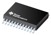
Datasheet Texas Instruments TPS65140PWPG4 — 数据表
| 制造商 | Texas Instruments |
| 系列 | TPS65140 |
| 零件号 | TPS65140PWPG4 |

具有全功能的4通道LCD偏置位置电荷泵,3.3V LDO控制,最小1.6A升压Ilim和故障检测24-HTSSOP -40至85
数据表
TPS6514x Triple Output LCD Supply With Linear Regulator and Power Good datasheet
PDF, 2.1 Mb, 修订版: F, 档案已发布: Jun 29, 2016
从文件中提取
价格
状态
| Lifecycle Status | Active (Recommended for new designs) |
| Manufacture's Sample Availability | No |
打包
| Pin | 24 |
| Package Type | PWP |
| Industry STD Term | HTSSOP |
| JEDEC Code | R-PDSO-G |
| Package QTY | 60 |
| Carrier | TUBE |
| Device Marking | TPS65140 |
| Width (mm) | 4.4 |
| Length (mm) | 7.8 |
| Thickness (mm) | 1 |
| Pitch (mm) | .65 |
| Max Height (mm) | 1.2 |
| Mechanical Data | 下载 |
参数化
| DisplayType | LCD Unipolar |
| IC Integration | LCD Bias |
| Level Shifter/Scan Driver | N/A Ch |
| Pin/Package | 24HTSSOP, 24VQFN |
| Source Driver Voltage(Max) | 15 V |
| Source Driver Voltage(Min) | 5 V |
| Special Function | N/A |
| Target Application | 7 to 13 inches,13 to 21 inches |
| Vin(Max) | 5.5 V |
| Vin(Min) | 2.7 V |
生态计划
| RoHS | Compliant |
设计套件和评估模块
- Evaluation Modules & Boards: TPS65130EVM-063
TPS65130 Evaluation Module
Lifecycle Status: Active (Recommended for new designs) - Evaluation Modules & Boards: TPS65140EVM-031
TPS65140 Evaluation Module
Lifecycle Status: Active (Recommended for new designs) - Evaluation Modules & Boards: TPS65100EVM-030
TPS65100 Evaluation Module
Lifecycle Status: Active (Recommended for new designs)
应用须知
- Customizing your TPS6510x/TPS6514XPDF, 233 Kb, 档案已发布: Jun 22, 2004
This application report shows how to use external circuitry to boost the output voltage capability of the positive and negative charge pumps of the TPS6510x and TPS6514x triple output power supplies. In addition the report shows how to use external circuitry to modify the internally controlled sequencing implement sequencing delay and short circuit protection. - How to Compensate the TPS6510x and the TPS6514xPDF, 1.1 Mb, 档案已发布: Aug 30, 2016
The boost converters in the TPS6510x (TPS65100 TPS65101 TPS65105) and the TPS6514x (TPS65140 TPS65141 TPS65145) series use external loop compensation providing high flexibility in LCD supply design. If designing a typical application scheme use the recommended components from the TPS6510x datasheet (SLVS496) and the TPS6514x datasheet (SLVS497). This application note gives a deeper understand - Basic Calculation of an Inverting Buck-Boost Power Stage (Rev. A)PDF, 431 Kb, 修订版: A, 档案已发布: Aug 28, 2017
This application note provides basic formulas that you need to design the power stage of an invertingbuck-boost converter. The premise is that the power switch is integrated in the IC and the rectification isdone by a diode (non-synchronous power stage). It provides all the formulas and considerations that youneed to select the external power components such as the inductor the diode and t - Generation of a VCOM buffer input using PWM signalPDF, 439 Kb, 档案已发布: Dec 21, 2015
In an LCD the backlight shines through the liquid crystal material and the voltage across the liquid crystal controls how much light shines through it. An active matrix LCD (AMLCD) contains many pixels arranged in a grid pattern. The voltage across each pixel is controlled individually so that high resolution images can be created. One terminal of every pixel is connected to a common plane. The v - Understanding Undervoltage Lockout in Power Devices (Rev. A)PDF, 90 Kb, 修订版: A, 档案已发布: Sep 19, 2018
Many integrated circuits include an undervoltage lockout (UVLO) function to disable the device at low supply voltages. Below the minimum supply voltage the function and performance of a device may be undefined making it impossible to predict system behavior. This application note explains how to correctly understand the undervoltage lockout specification in the data sheets of TI's power products. - Minimizing Ringing at the Switch Node of a Boost ConverterPDF, 201 Kb, 档案已发布: Sep 15, 2006
The application report explains how to use proper board layout and/or a snubber to reduce high-frequency ringing at the switch node of a boost converter. - Basic Calculation of a Boost Converter's Power Stage (Rev. C)PDF, 186 Kb, 修订版: C, 档案已发布: Jan 8, 2014
This application note gives the equations to calculate the power stage of a boost converter built with an IC with integrated switch and operating in continuous conduction mode. It is not intended to give details on the functionality of a boost converter (see Reference 1) or how to compensate a converter. See the references at the end of this document if more detail is needed.
模型线
系列: TPS65140 (4)
- TPS65140PWP TPS65140PWPG4 TPS65140PWPR TPS65140RGER
制造商分类
- Semiconductors > Power Management > LCD/OLED Display Bias Solutions