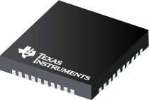
Datasheet Texas Instruments TPS65155RKPR — 数据表
| 制造商 | Texas Instruments |
| 系列 | TPS65155 |
| 零件号 | TPS65155RKPR |

带有电平转换器的LCD偏置解决方案,用于GOA面板40-VQFN -40至85
数据表
价格
状态
| Lifecycle Status | Active (Recommended for new designs) |
| Manufacture's Sample Availability | Yes |
打包
| Pin | 40 |
| Package Type | RKP |
| Industry STD Term | VQFN |
| JEDEC Code | S-PQFP-N |
| Package QTY | 3000 |
| Carrier | LARGE T&R |
| Width (mm) | 5 |
| Length (mm) | 5 |
| Thickness (mm) | 0.9 |
| Pitch (mm) | 0.4 |
| Max Height (mm) | 1 |
| Mechanical Data | 下载 |
参数化
| DisplayType | LCD Unipolar |
| IC Integration | LCD Bias,LCD Level shifter |
| Level Shifter/Scan Driver | 6 Ch |
| Pin/Package | 40VQFN |
| Source Driver Voltage(Max) | 18 V |
| Source Driver Voltage(Min) | 7 V |
| Special Function | I2C I/F,Level Shifter,Output Discharge,Reset Generator,Temperature Sensor/Compensation |
| Target Application | 13 to 21 inches,7 to 13 inches |
| Topology | Boost |
| Vin(Max) | 6 V |
| Vin(Min) | 3 V |
生态计划
| RoHS | Compliant |
应用须知
- Generation of a VCOM buffer input using PWM signalPDF, 439 Kb, 档案已发布: Dec 21, 2015
In an LCD the backlight shines through the liquid crystal material and the voltage across the liquid crystal controls how much light shines through it. An active matrix LCD (AMLCD) contains many pixels arranged in a grid pattern. The voltage across each pixel is controlled individually so that high resolution images can be created. One terminal of every pixel is connected to a common plane. The v - Understanding Undervoltage Lockout in Power Devices (Rev. A)PDF, 90 Kb, 修订版: A, 档案已发布: Sep 19, 2018
Many integrated circuits include an undervoltage lockout (UVLO) function to disable the device at low supply voltages. Below the minimum supply voltage the function and performance of a device may be undefined making it impossible to predict system behavior. This application note explains how to correctly understand the undervoltage lockout specification in the data sheets of TI's power products. - Minimizing Ringing at the Switch Node of a Boost ConverterPDF, 201 Kb, 档案已发布: Sep 15, 2006
The application report explains how to use proper board layout and/or a snubber to reduce high-frequency ringing at the switch node of a boost converter. - Basic Calculation of a Boost Converter's Power Stage (Rev. C)PDF, 186 Kb, 修订版: C, 档案已发布: Jan 8, 2014
This application note gives the equations to calculate the power stage of a boost converter built with an IC with integrated switch and operating in continuous conduction mode. It is not intended to give details on the functionality of a boost converter (see Reference 1) or how to compensate a converter. See the references at the end of this document if more detail is needed.
模型线
系列: TPS65155 (1)
- TPS65155RKPR
制造商分类
- Semiconductors > Power Management > LCD/OLED Display Bias Solutions