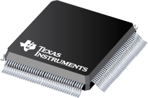
TMS320VC5410 Fixed-Point
Digital Signal Processor
Data Manual Literature Number: SPRS075E
October 1998 -Revised December 2000 PRODUCTION DATA information is current as of publication date.
Products conform to specifications per the terms of Texas Instruments
standard warranty. Production processing does not necessarily include
testing of all parameters. (This page has been left blank intentionally.) REVISION HISTORY
REVISION DATE PRODUCT STATUS HIGHLIGHTS * October 1998 Advance Information Original A February 1999 Advance Information Updated characteristic data B June 1999 Production Data Updated characteristic data C January 2000 Production Data Updated characteristic data D May 2000 Production Data Updated characteristic data E November 2000 Production Data 1. Converted from data sheet format to data manual format. 2. Removed the TMS320VC5410-120 from this datasheet and created a
separate document (literature number SPRS158) This affectes several places
in this document. 3. Corrected: 4. Maximum disable time of the BDX signal with external BCLKX in the
switching characteristics table of McBSP serial port timing section.
Improved timing diagrams (Figure 4-21, and Figure 4-22) in the McBSP
serial port timing section. Minimum high-level input voltage (VIHmin) for the HPI databus signals,
HD[7:0] from 2 V to 2.2 V in the recommended operating conditions. Minimum cycle time of CLKOUT in the switching characteristics table of
the divide-by-clock option. Minimum cycle time of X2/CLKIN in the timing requirements table of the
divide-by-two clock option. Maximum rise and fall times of X2/CLKIN in the timing requirements table
of the divide-by-two clock option. Minimum and maximum cycle times for X2/CLKIN in the timing
requirements table of the multiply-by-N clcok option. Several timing values in the switching characteristics table of the HPI8
timing section. Added: Clarifying paragraph to Section 4.14.1 “McBSP Transmit and Receive
Timings”, regarding the effect of the CLKOUT divide factor on the serial
port timings. BCLKS timings to the timing requirements table, switching
characteristics table, and timing diagrams of the McBSP serial port timing
section. Clarifying sentence to Table 2-4. “Bank-Switching Control Register …
