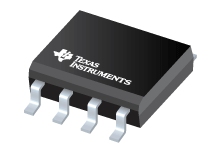
Datasheet Texas Instruments OPA698IDG4 — 数据表
| 制造商 | Texas Instruments |
| 系列 | OPA698 |
| 零件号 | OPA698IDG4 |

单位增益稳定的宽带电压限制放大器8-SOIC -40至85
数据表
Unity Gain Stable, Wideband Voltage Limiting Amplifier datasheet
PDF, 837 Kb, 修订版: D, 档案已发布: Dec 30, 2008
从文件中提取
价格
状态
| Lifecycle Status | Active (Recommended for new designs) |
| Manufacture's Sample Availability | Yes |
打包
| Pin | 8 | 8 |
| Package Type | D | D |
| Industry STD Term | SOIC | SOIC |
| JEDEC Code | R-PDSO-G | R-PDSO-G |
| Package QTY | 75 | 75 |
| Carrier | TUBE | TUBE |
| Device Marking | 698 | OPA |
| Width (mm) | 3.91 | 3.91 |
| Length (mm) | 4.9 | 4.9 |
| Thickness (mm) | 1.58 | 1.58 |
| Pitch (mm) | 1.27 | 1.27 |
| Max Height (mm) | 1.75 | 1.75 |
| Mechanical Data | 下载 | 下载 |
参数化
| 2nd Harmonic | 74 dBc |
| 3rd Harmonic | 87 dBc |
| @ MHz | 5 |
| Acl, min spec gain | 1 V/V |
| Additional Features | N/A |
| Architecture | Voltage FB |
| BW @ Acl | 450 MHz |
| CMRR(Min) | 54 dB |
| CMRR(Typ) | 61 dB |
| GBW(Typ) | 250 MHz |
| Input Bias Current(Max) | 10000000 pA |
| Iq per channel(Max) | 15.9 mA |
| Iq per channel(Typ) | 15.5 mA |
| Number of Channels | 1 |
| Offset Drift(Typ) | 15 uV/C |
| Operating Temperature Range | -40 to 85 C |
| Output Current(Typ) | 120 mA |
| Package Group | SOIC |
| Package Size: mm2:W x L | 8SOIC: 29 mm2: 6 x 4.9(SOIC) PKG |
| Rail-to-Rail | No |
| Rating | Catalog |
| Slew Rate(Typ) | 1100 V/us |
| Total Supply Voltage(Max) | 12 +5V=5, +/-5V=10 |
| Total Supply Voltage(Min) | 5 +5V=5, +/-5V=10 |
| Vn at 1kHz(Typ) | 11 nV/rtHz |
| Vn at Flatband(Typ) | 5.6 nV/rtHz |
| Vos (Offset Voltage @ 25C)(Max) | 6 mV |
生态计划
| RoHS | Compliant |
设计套件和评估模块
- Evaluation Modules & Boards: DEM-OPA-SO-1A
DEM-OPA-SO-1A Unpopulated PCB Compatible w/High Speed Wide Bandwidth Op Amps in 8-lead SOIC (D) Pkg
Lifecycle Status: Active (Recommended for new designs)
应用须知
- ADC Input ProtectionPDF, 145 Kb, 档案已发布: Sep 4, 2013
- Video Designs Using High-Speed Amplifiers (Rev. A)PDF, 438 Kb, 修订版: A, 档案已发布: Feb 3, 2005
- RLC Filter Design for ADC Interface Applications (Rev. A)PDF, 299 Kb, 修订版: A, 档案已发布: May 13, 2015
As high performance Analog-to-Digital Converters (ADCs) continue to improve in their performance, the last stage interface from the final amplifier into the converter inputs becomes a critical element in the system design if the full converter dynamic range is desired. This application note describes the performance and design equations for a simple passive 2nd-order filter used successfully in AD - ADS5500, OPA695: PC Board Layout for Low Distortion High-Speed ADC DriversPDF, 273 Kb, 档案已发布: Apr 22, 2004
Once an analog-to-digital converter (ADC) and a driver/interface have been selected for a given application, the next step to achieving excellent performance is laying out the printed circuit board (PCB) that will support the application. This application report describes several techniques for optimizing a high-speed, 14-bit performance, differential driver PCB layout using a wideband operation - Measuring Board Parasitics in High-Speed Analog DesignPDF, 134 Kb, 档案已发布: Jul 7, 2003
Successful circuit designs using high-speed amplifiers can depend upon understanding and identifying parasitic PCB components. Simulating a design while including PCB parasitics can protect against unpleasant production surprises. This application report discusses an easy method for measuring parasitic components in a prototype or final PC board design by using a standard oscilloscope and low freq - Noise Analysis for High Speed Op Amps (Rev. A)PDF, 256 Kb, 修订版: A, 档案已发布: Jan 17, 2005
As system bandwidths have increased an accurate estimate of the noise contribution for each element in the signal channel has become increasingly important. Many designers are not however particularly comfortable with the calculations required to predict the total noise for an op amp or in the conversions between the different descriptions of noise. Considerable inconsistency between manufactu
模型线
系列: OPA698 (4)
- OPA698ID OPA698IDG4 OPA698IDR OPA698IDRG4
制造商分类
- Semiconductors > Amplifiers > Operational Amplifiers (Op Amps) > High-Speed Op Amps (>=50MHz)