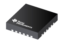
Datasheet Texas Instruments TPS65130RGER — 数据表
| 制造商 | Texas Instruments |
| 系列 | TPS65130 |
| 零件号 | TPS65130RGER |

具有双正输出和负输出(典型值为200mA)的24VQFN分离轨转换器-40至85
数据表
TPS6513x Positive and Negative Output DC-DC Converter datasheet
PDF, 1.8 Mb, 修订版: D, 档案已发布: Jan 26, 2016
从文件中提取
价格
状态
| Lifecycle Status | Active (Recommended for new designs) |
| Manufacture's Sample Availability | Yes |
打包
| Pin | 24 | 24 |
| Package Type | RGE | RGE |
| Industry STD Term | VQFN | VQFN |
| JEDEC Code | S-PQFP-N | S-PQFP-N |
| Package QTY | 3000 | 3000 |
| Carrier | LARGE T&R | LARGE T&R |
| Device Marking | 5130 | TPS6 |
| Width (mm) | 4 | 4 |
| Length (mm) | 4 | 4 |
| Thickness (mm) | .88 | .88 |
| Pitch (mm) | .5 | .5 |
| Max Height (mm) | 1 | 1 |
| Mechanical Data | 下载 | 下载 |
参数化
| Iout(Max) | 0.3 A |
| Iq(Typ) | 0.5 mA |
| Operating Temperature Range | -40 to 85 C |
| Package Group | VQFN |
| Rating | Catalog |
| Switching Frequency(Max) | 1500 kHz |
| Switching Frequency(Min) | 1250 kHz |
| Topology | Split-Rail |
| Type | Converter |
| Vin(Max) | 5.5 V |
| Vin(Min) | 2.7 V |
| Vout(Max) | 15 V |
| Vout(Min) | 3.2 V |
| Vout2(Max) | -2 V |
| Vout2(Min) | -15 V |
生态计划
| RoHS | Compliant |
设计套件和评估模块
- Evaluation Modules & Boards: TPS65130EVM-063
TPS65130 Evaluation Module
Lifecycle Status: Active (Recommended for new designs)
应用须知
- Basic Calculation of an Inverting Buck-Boost Power Stage (Rev. A)PDF, 431 Kb, 修订版: A, 档案已发布: Aug 28, 2017
This application note provides basic formulas that you need to design the power stage of an invertingbuck-boost converter. The premise is that the power switch is integrated in the IC and the rectification isdone by a diode (non-synchronous power stage). It provides all the formulas and considerations that youneed to select the external power components such as the inductor the diode and t - Understanding Undervoltage Lockout in Power Devices (Rev. A)PDF, 90 Kb, 修订版: A, 档案已发布: Sep 19, 2018
Many integrated circuits include an undervoltage lockout (UVLO) function to disable the device at low supply voltages. Below the minimum supply voltage the function and performance of a device may be undefined making it impossible to predict system behavior. This application note explains how to correctly understand the undervoltage lockout specification in the data sheets of TI's power products. - Minimizing Ringing at the Switch Node of a Boost ConverterPDF, 201 Kb, 档案已发布: Sep 15, 2006
The application report explains how to use proper board layout and/or a snubber to reduce high-frequency ringing at the switch node of a boost converter. - Basic Calculation of a Boost Converter's Power Stage (Rev. C)PDF, 186 Kb, 修订版: C, 档案已发布: Jan 8, 2014
This application note gives the equations to calculate the power stage of a boost converter built with an IC with integrated switch and operating in continuous conduction mode. It is not intended to give details on the functionality of a boost converter (see Reference 1) or how to compensate a converter. See the references at the end of this document if more detail is needed. - Basic Calculation of a Buck Converter's Power Stage (Rev. B)PDF, 202 Kb, 修订版: B, 档案已发布: Aug 17, 2015
模型线
系列: TPS65130 (4)
- TPS65130RGER TPS65130RGERG4 TPS65130RGET TPS65130RGETG4
制造商分类
- Semiconductors > Power Management > Non-isolated DC/DC Switching Regulator > Buck/Boost, Inverting or Split-Rail > Buck/Boost, Inverting or Split-Rail Converter (Integrated Switch)